- 您现在的位置:买卖IC网 > Sheet目录366 > TMDXEVM5515 (Texas Instruments)EVAL MODULE DSP FOR C55XX
�� ��
��
��SPRS645F� –� AUGUST� 2010� –� REVISED� OCTOBER� 2013�
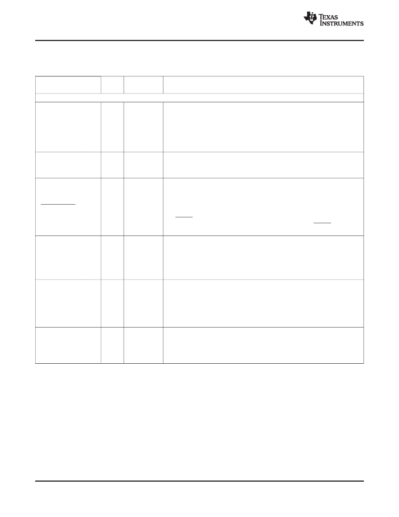
�2.5.14� Regulators� and� Power� Management� Terminal� Functions�
�Table� 2-19.� Regulators� and� Power� Management� Terminal� Functions�
��SIGNAL�
�NAME�
�NO.�
�TYPE� (1)�
�(2)�
�OTHER� (3)�
�(4)�
�DESCRIPTION�
�Regulators�
�DSP_LDO� output.� When� enabled,� this� output� provides� a� regulated� 1.3� V� or� 1.05� V�
�output� and� up� to� 250� mA� of� current� (see� the� I� SD� parameter� in� Section� 4.3� ,� Electrical�
�Characteristics� Over� Recommended� Ranges� of� Supply� Voltage� and� Operating�
�DSP_LDOO�
�E10�
�S�
�Temperature).� The� DSP_LDO� is� intended� to� supply� current� to� the� digital� core� circuits�
�only� (CV� DD� )� and� not� external� devices.� For� proper� device� operation,� the� external�
�decoupling� capacitor� of� this� pin� should� be� 5μF� ~� 10μF.� For� more� detailed�
�information,� see� Section� 5.3.4� ,� Power-Supply� Decoupling� .�
�When� disabled,� this� pin� is� in� the� high-impedance� (Hi-Z)� state.�
�LDOI�
�F14,�
�F13,�
�B12�
�S�
�LDO� inputs.� For� proper� device� operation,� LDOI� must� always� be� powered.� The� LDOI�
�pins� must� be� connected� to� the� same� power� supply� source� with� a� voltage� range� of�
�1.8� V� to� 3.6� V.� These� pins� supply� power� to� the� internal� LDOs,� the� bandgap�
�reference� generator� circuits,� and� serve� as� the� I/O� supply� for� some� input� pins.�
�DSP_LDO� enable� input.� This� signal� is� not� intended� to� be� dynamically� switched.�
�0� =� DSP_LDO� is� enabled.� The� internal� POR� monitors� the� DSP_LDOO� pin� voltage�
�and� generates� the� internal� POWERGOOD� signal.�
�DSP_LDO_EN�
�D12�
�I�
�–�
�LDOI�
�1� =� DSP_LDO� is� disabled.� The� internal� POR� voltage� monitoring� is� also� disabled.�
�The� interna� l� POWERGOOD� signal� is� forced� high� and� the� external� reset� signal� on�
�the� RESET� pin� (D6)� is� the� only� source� of� the� device� reset.� Note,� the� device's�
�internal� reset� signal� is� generated� as� the� logical� AND� of� the� RESET� pin� and� the�
�internal� POWERGOOD� signal.�
�USB_LDO� output.� This� output� provides� a� regulated� 1.3� V� output� and� up� to� 25� mA� of�
�current� (see� the� I� SD� parameter� in� Section� 4.3� ,� Electrical� Characteristics� Over�
�Recommended� Ranges� of� Supply� Voltage� and� Operating� Temperature).� For� proper�
�USB_LDOO�
�F12�
�S�
�device� operation,� this� pin� must� be� connected� to� a� 1� μ� F� ~� 2� μ� F� decoupling� capacitor�
�to� V� SS� .� For� more� detailed� information,� see� Section� 5.3.4� ,� Power-Supply� Decoupling� .�
�This� LDO� is� intended� to� supply� power� to� the� USB_� V� DD1P3� ,� USB_V� DDA1P3� pins� and�
�not� external� devices.�
�ANA_LDO� output.� This� output� provides� a� regulated� 1.3� V� output� and� up� to� 4� mA� of�
�current� (see� the� I� SD� parameter� in� Section� 4.3� ,� Electrical� Characteristics� Over�
�Recommended� Ranges� of� Supply� Voltage� and� Operating� Temperature� ).�
�ANA_LDOO�
�A12�
�S�
�For� proper� device� operation,� this� pin� must� be� connected� to� an� ~� 1.0� μ� F� decoupling�
�capacitor� to� V� SS� .� For� more� detailed� information,� see� Section� 5.3.4� ,� Power-Supply�
�Decoupling� .� This� LDO� is� intended� to� supply� power� to� the� V� DDA_ANA� and� V� DDA_PLL�
�pins� and� not� external� devices.�
�Bandgap� reference� filter� signal.� For� proper� device� operation,� this� pin� needs� to� be�
�bypassed� with� a� 0.1� μ� F� capacitor� to� analog� ground� (V� SSA_ANA� ).�
�BG_CAP�
�B13�
�A,� I/O�
�This� external� capacitor� provides� filtering� for� stable� reference� voltages� &� currents�
�generated� by� the� bandgap� circuit.� The� bandgap� produces� the� references� for� use� by�
�the� System� PLL,� SAR,� and� POR� circuits.�
�(1)�
�(2)�
�(3)�
�(4)�
�I� =� Input,� O� =� Output,� Z� =� High� impedance,� S� =� Supply� voltage,� GND� =� Ground,� A� =� Analog� signal,� BH� =� Bus� Holder�
�Input� pins� of� type� I,� I/O,� and� I/O/Z� are� required� to� be� driven� at� all� times.� To� achieve� the� lowest� power,� these� pins� must� not� be� allowed� to�
�float.� When� they� are� configured� as� input� or� high-impedance� state,� and� not� driven� to� a� known� state,� they� may� cause� an� excessive� IO-�
�supply� current.� Prevent� this� current� by� externally� terminating� it� or� enabling� IPD/IPU,� if� applicable.�
�IPD� =� Internal� pulldown,� IPU� =� Internal� pullup.� For� more� detailed� information� on� pullup/pulldown� resistors� and� situations� where� external�
�pullup/pulldown� resistors� are� required,� see� Section� 3.8.1� ,� Pullup/Pulldown� Resistors� .�
�Specifies� the� operating� I/O� supply� voltage� for� each� signal�
�42�
�Device� Overview�
��Product� Folder� Links:� TMS320C5515�
�Copyright� ?� 2010–2013,� Texas� Instruments� Incorporated�
�发布紧急采购,3分钟左右您将得到回复。
相关PDF资料
TMDXEXP1808L
KIT EXPERIMENTER FOR AM180X
TO263-3EV-VREG
BOARD EVAL TO220-3/TO263-3 VREG
TO263-5EV-VREG
EVAL BOARD VREG TO220-5/TO263-5
TOOLSTICK-EK
KIT TOOL EVAL SYS IN A USB STICK
TPS23757EVM
EVALUATION MODULE FOR TPS23757
TPS62230EVM-370
EVAL MODULE FOR TPS62230-370
TRAVELCUBE
SURGE SUP 1OUT W/RJ11 DIRECTPLUG
TRAVELER100BT
SURGE SUP 2OUT W/RJ11 DIRECTPLUG
相关代理商/技术参数
TMDXEVM5515
制造商:Texas Instruments 功能描述:TMS320C5515 DSP Evaluation Module
TMDXEVM642
制造商:Texas Instruments 功能描述:Tools Development kit For Use
TMDXEVM6424
功能描述:开发板和工具包 - TMS320 C6424 DSP Eval Mod RoHS:否 制造商:Texas Instruments 产品:Experimenter Kits 工具用于评估:F2802x 核心:TMS320 接口类型:UART, USB 工作电源电压:
TMDXEVM6446
制造商:Rochester Electronics LLC 功能描述:DAVINCI EVM BUNDLE W/O EMULATOR - Bulk 制造商:Texas Instruments 功能描述:DAVINCI EVM BUNDLE W/O EMULATOR - Bulk
TMDXEVM6446T
制造商:Texas Instruments 功能描述:DM6446 DIGITAL VIDEO EVALUATION MODULE - Boxed Product (Development Kits)
TMDXEVM6446TS
制造商:Texas Instruments 功能描述:DM6446 DIGITAL VIDEO EVALUATION MODULE - Trays
TMDXEVM6452
功能描述:开发板和工具包 - TMS320 C6452 EVM Evaluation Module RoHS:否 制造商:Texas Instruments 产品:Experimenter Kits 工具用于评估:F2802x 核心:TMS320 接口类型:UART, USB 工作电源电压:
TMDXEVM6455
功能描述:开发板和工具包 - TMS320 C6455 Evaluation Module RoHS:否 制造商:Texas Instruments 产品:Experimenter Kits 工具用于评估:F2802x 核心:TMS320 接口类型:UART, USB 工作电源电压: